

What is the effect of Five Layers Vertical Plasma Equipment on the electrical conductivity of processed materials?
Jan 16, 2026
The electrical conductivity of materials is a crucial property that determines their performance in various applications, especially in the electronics industry. As a supplier of Five Layers Vertical Plasma Equipment, I have witnessed firsthand the transformative impact of this advanced technology on the electrical conductivity of processed materials. In this blog post, I will delve into the effects of our Five Layers Vertical Plasma Equipment on the electrical conductivity of materials, exploring the underlying mechanisms and real-world applications.
Understanding Plasma Treatment and Electrical Conductivity
Before we discuss the specific effects of our Five Layers Vertical Plasma Equipment, it is essential to understand the basics of plasma treatment and its relationship with electrical conductivity. Plasma is often referred to as the fourth state of matter, consisting of ions, electrons, and neutral particles. Plasma treatment involves exposing materials to a plasma environment, which can modify the surface properties of the material through various physical and chemical processes.
Electrical conductivity, on the other hand, is a measure of a material's ability to conduct an electric current. It is determined by the presence and mobility of charge carriers, such as electrons or ions, within the material. In many cases, the surface properties of a material can significantly influence its electrical conductivity, as the surface is often the interface through which charge carriers interact with the external environment.

How Five Layers Vertical Plasma Equipment Affects Electrical Conductivity
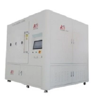
Our Five Layers Vertical Plasma Equipment is designed to provide a highly controlled and efficient plasma treatment process. The equipment features a unique five-layer vertical structure, which allows for precise control of the plasma environment and ensures uniform treatment across the entire surface of the material. Here are some of the key ways in which our equipment can affect the electrical conductivity of processed materials:
Surface Cleaning and Activation
One of the primary functions of plasma treatment is to clean and activate the surface of the material. During the plasma treatment process, the high-energy ions and radicals in the plasma can remove contaminants, such as organic residues and oxides, from the material's surface. This cleaning effect can improve the electrical contact between the material and other components, thereby enhancing the overall electrical conductivity.
In addition to cleaning, plasma treatment can also activate the surface of the material by creating reactive functional groups. These functional groups can promote chemical bonding between the material and other substances, such as conductive polymers or metal coatings. By improving the adhesion between the material and conductive layers, the plasma treatment can further enhance the electrical conductivity of the material.
Surface Modification and Doping
Another way in which our Five Layers Vertical Plasma Equipment can affect electrical conductivity is through surface modification and doping. The plasma treatment process can introduce foreign atoms or molecules into the material's surface, a process known as doping. Doping can alter the electronic structure of the material and increase the concentration of charge carriers, thereby improving the electrical conductivity.
For example, in the case of semiconductor materials, plasma doping can be used to introduce impurities that create additional charge carriers, such as electrons or holes. This can significantly enhance the electrical conductivity of the semiconductor and improve its performance in electronic devices.
Formation of Conductive Layers
Our Five Layers Vertical Plasma Equipment can also be used to deposit conductive layers on the surface of the material. Through a process known as plasma-enhanced chemical vapor deposition (PECVD), the equipment can create thin films of conductive materials, such as metals or conductive polymers, on the material's surface. These conductive layers can provide an additional pathway for the flow of electric current, thereby increasing the overall electrical conductivity of the material.
The PECVD process in our equipment is highly controllable, allowing for precise control of the thickness, composition, and morphology of the conductive layers. This ensures that the deposited layers have optimal electrical properties and are well-suited for specific applications.
Real-World Applications
The ability of our Five Layers Vertical Plasma Equipment to improve the electrical conductivity of materials has a wide range of real-world applications. Here are some examples:
Printed Circuit Boards (PCBs)
PCBs are essential components in electronic devices, providing a platform for the interconnection of electronic components. Our PCB Vertical Plasma Equipment, which is based on the same five-layer vertical plasma technology, can be used to improve the electrical conductivity of PCB substrates. By cleaning and activating the surface of the PCB, the plasma treatment can enhance the adhesion between the copper traces and the substrate, reducing the resistance and improving the signal transmission performance.
Flexible Electronics
Flexible electronics are a rapidly growing field, with applications in wearable devices, flexible displays, and smart sensors. Our Five Layers Vertical Plasma Equipment can be used to treat flexible substrates, such as polymers and plastics, to improve their electrical conductivity. By depositing conductive layers or doping the surface of the substrate, the plasma treatment can enable the development of high-performance flexible electronic devices.
Energy Storage Devices
Energy storage devices, such as batteries and supercapacitors, require materials with high electrical conductivity to ensure efficient charge and discharge processes. Our equipment can be used to treat electrode materials, such as carbon-based materials and metal oxides, to improve their electrical conductivity. This can enhance the performance and lifespan of energy storage devices, making them more suitable for various applications, including electric vehicles and renewable energy systems.
Comparing with Other Plasma Equipment
While there are other types of plasma equipment available on the market, our Five Layers Vertical Plasma Equipment offers several advantages in terms of its impact on electrical conductivity:
Uniform Treatment
The unique five-layer vertical structure of our equipment ensures uniform plasma distribution across the entire surface of the material. This results in consistent treatment and improved electrical conductivity across the material, which is particularly important for large-area applications.
Precise Control
Our equipment allows for precise control of the plasma parameters, such as power, pressure, and gas composition. This level of control enables us to tailor the plasma treatment process to the specific requirements of the material and application, ensuring optimal results in terms of electrical conductivity improvement.
High Efficiency
The vertical design of our equipment allows for a compact and efficient plasma treatment process. This reduces the treatment time and energy consumption, making our equipment a cost-effective solution for improving the electrical conductivity of materials.
Conclusion
In conclusion, our Five Layers Vertical Plasma Equipment offers a powerful and versatile solution for improving the electrical conductivity of processed materials. Through surface cleaning, activation, modification, and deposition, the equipment can significantly enhance the electrical properties of materials, opening up new possibilities for a wide range of applications in the electronics, energy, and other industries.
If you are interested in learning more about our Five Layers Vertical Plasma Equipment or exploring how it can be used to improve the electrical conductivity of your materials, please feel free to contact us. We are committed to providing high-quality plasma treatment solutions and look forward to discussing your specific needs and requirements.
References
- Smith, J. (2018). Plasma Surface Treatment: Principles and Applications. Wiley.
- Chen, X., & Wang, Y. (2020). Advances in Plasma-Enhanced Nanomaterial Synthesis for Energy and Environmental Applications. Chemical Reviews, 120(17), 8736-8812.
- Zhang, L., & Li, H. (2019). Plasma Treatment for Flexible Electronics: A Review. Journal of Materials Chemistry C, 7(39), 12155-12172.