

How does LED RF Plasma Equipment treat LED surfaces?
Jul 31, 2026
LED technology has witnessed remarkable growth in recent years, with applications spanning from lighting solutions to displays and automotive lighting. However, to ensure optimal performance and reliability, surface treatment of LEDs is crucial. This is where LED RF Plasma Equipment comes into play. As a leading supplier of LED RF Plasma Equipment, we understand the significance of this technology in enhancing the surface properties of LEDs. In this blog, we will delve into how our LED RF Plasma Equipment treats LED surfaces and the benefits it offers.
Understanding RF Plasma Technology
RF (Radio Frequency) plasma is a state of matter where a gas is ionized to create a mixture of ions, electrons, and neutral particles. This highly reactive environment can be harnessed to modify the surface properties of materials. In the context of LED manufacturing, RF plasma technology is used to clean, activate, and coat the surfaces of LEDs.
Our LED RF Plasma Equipment generates RF plasma by applying a high-frequency electromagnetic field to a gas, typically argon or oxygen. The gas molecules are ionized, creating a plasma that can interact with the LED surface. The plasma can remove contaminants, such as organic residues and oxides, from the surface, improving the adhesion of subsequent coatings or bonding processes. It can also activate the surface by creating reactive sites, which enhances the chemical reactivity of the LED surface.
Surface Cleaning
One of the primary functions of our LED RF Plasma Equipment is surface cleaning. During the manufacturing process, LEDs can accumulate various contaminants on their surfaces, including dust, grease, and organic residues. These contaminants can affect the performance and reliability of the LEDs, such as reducing the light output or causing electrical shorts.
Our RF plasma cleaning process uses a combination of physical and chemical reactions to remove these contaminants. The high-energy ions in the plasma bombard the surface, physically dislodging the contaminants. At the same time, the reactive species in the plasma, such as oxygen radicals, can react with the organic contaminants, breaking them down into volatile compounds that can be easily removed from the chamber.
The benefits of surface cleaning using our LED RF Plasma Equipment are significant. It ensures a clean and uniform surface, which is essential for subsequent processes such as die bonding and wire bonding. By removing contaminants, the adhesion between the LED and the substrate or other components is improved, reducing the risk of delamination or failure. Additionally, a clean surface can enhance the light extraction efficiency of the LED, resulting in higher brightness and better performance.
Surface Activation
In addition to cleaning, our LED RF Plasma Equipment can also activate the LED surface. Surface activation involves creating reactive sites on the surface, which can improve the chemical reactivity of the LED. This is particularly important for processes such as coating deposition or bonding, where strong adhesion between the LED and the coating or bonding material is required.
Our RF plasma activation process modifies the surface chemistry of the LED by introducing functional groups such as hydroxyl (-OH) or carbonyl (-C=O) groups. These functional groups can react with the coating or bonding material, forming strong chemical bonds. The activation process can also increase the surface energy of the LED, which improves the wetting properties of the surface and enhances the spreading of the coating or bonding material.
The benefits of surface activation are evident in improved adhesion and reliability. By creating a more reactive surface, the LED can form stronger bonds with the coating or bonding material, reducing the risk of delamination or failure. This is particularly important in applications where the LED is exposed to harsh environmental conditions, such as high temperatures or humidity. Additionally, surface activation can improve the performance of the LED by enhancing the light extraction efficiency or reducing the electrical resistance.
Surface Coating
Our LED RF Plasma Equipment can also be used for surface coating applications. Surface coating can provide additional protection to the LED, improve its performance, or enhance its aesthetic appearance. Common coating materials used in LED manufacturing include silicon dioxide (SiO2), titanium dioxide (TiO2), and aluminum oxide (Al2O3).
The RF plasma coating process involves depositing a thin layer of the coating material onto the LED surface. The coating material is typically introduced into the plasma chamber in the form of a gas or vapor. The high-energy ions in the plasma can break down the coating material into smaller particles, which can then deposit onto the LED surface. The plasma can also assist in the chemical reaction between the coating material and the LED surface, forming a strong bond.
The benefits of surface coating using our LED RF Plasma Equipment are numerous. A protective coating can prevent the LED from being damaged by environmental factors such as moisture, oxygen, or UV radiation. It can also improve the thermal conductivity of the LED, which helps to dissipate heat more effectively and reduce the risk of overheating. Additionally, a coating can enhance the light extraction efficiency of the LED by reducing the reflection of light at the surface.
Types of LED RF Plasma Equipment
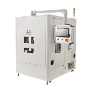
As a supplier of LED RF Plasma Equipment, we offer a range of products to meet the diverse needs of our customers. Our product portfolio includes Vacuum Inline RF Plasma Equipment, LCD RF Plasma Equipment, and RF Plasma Equipment for Semiconductor Applications.
Our Vacuum Inline RF Plasma Equipment is designed for high-volume production environments. It features a continuous inline processing system, which allows for efficient and automated surface treatment of LEDs. The equipment can be integrated into existing production lines, minimizing downtime and maximizing productivity.
Our LCD RF Plasma Equipment is specifically designed for the treatment of LCD panels and other flat panel displays. It offers precise control over the plasma parameters, ensuring uniform treatment across the entire surface of the panel. The equipment can be used for cleaning, activation, and coating applications, improving the performance and reliability of the LCD.
Our RF Plasma Equipment for Semiconductor Applications is suitable for the treatment of semiconductor wafers and other electronic components. It offers high-performance plasma generation and control, enabling precise surface modification and treatment. The equipment can be used for a variety of applications, including surface cleaning, activation, and etching.
Conclusion
In conclusion, our LED RF Plasma Equipment plays a crucial role in the surface treatment of LEDs. By providing surface cleaning, activation, and coating capabilities, our equipment can improve the performance, reliability, and aesthetics of the LEDs. The benefits of using our equipment include improved adhesion, enhanced light extraction efficiency, and better protection against environmental factors.

As a leading supplier of LED RF Plasma Equipment, we are committed to providing our customers with high-quality products and excellent service. Our team of experts can help you select the right equipment for your specific needs and provide technical support and training. If you are interested in learning more about our LED RF Plasma Equipment or would like to discuss your surface treatment requirements, please contact us. We look forward to the opportunity to work with you and help you achieve your goals in LED manufacturing.
References
- "Plasma Surface Treatment for LED Packaging" by X. Wang et al., Journal of Display Technology, Vol. 10, No. 12, 2014.
- "Surface Modification of LEDs Using RF Plasma" by Y. Zhang et al., Applied Surface Science, Vol. 257, No. 12, 2011.
- "Plasma Technology in Semiconductor Manufacturing" by S. M. Rossnagel, IEEE Transactions on Plasma Science, Vol. 29, No. 6, 2001.