

Can Vacuum Inline RF Plasma Equipment be used for semiconductor manufacturing?
Jul 23, 2026
Vacuum inline RF plasma equipment has emerged as a powerful tool in various industrial applications, and one of the most significant areas of interest is semiconductor manufacturing. As a supplier of Vacuum Inline RF Plasma Equipment, I am often asked whether this technology can be effectively used in semiconductor production. In this blog, we will explore the capabilities of vacuum inline RF plasma equipment and its potential applications in the semiconductor industry.
Understanding Vacuum Inline RF Plasma Equipment
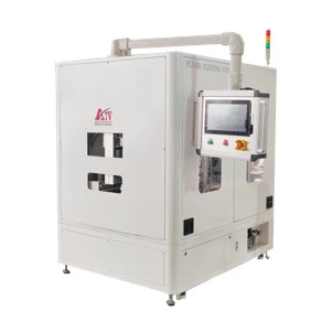
Before delving into its applications in semiconductor manufacturing, it is essential to understand what vacuum inline RF plasma equipment is. This equipment utilizes radio frequency (RF) energy to generate a plasma within a vacuum chamber. Plasma is a state of matter consisting of ions, electrons, and neutral particles. The RF energy excites the gas molecules in the chamber, creating a plasma that can be used for various surface treatment processes.
The "inline" aspect of the equipment refers to its ability to be integrated into a production line. This allows for continuous processing of semiconductor wafers or other substrates, increasing efficiency and throughput. The vacuum environment ensures that the plasma treatment is carried out in a clean and controlled manner, minimizing the risk of contamination.
Surface Cleaning and Activation
One of the primary applications of vacuum inline RF plasma equipment in semiconductor manufacturing is surface cleaning and activation. Semiconductor wafers often have contaminants on their surfaces, such as organic residues, oxides, and particles. These contaminants can affect the performance and reliability of the semiconductor devices.
Plasma cleaning uses the reactive species in the plasma, such as ions and radicals, to remove these contaminants. For example, oxygen plasma can be used to oxidize and remove organic residues, while argon plasma can be used for sputtering and removing particles. The plasma treatment not only cleans the surface but also activates it, increasing the surface energy and improving the adhesion of subsequent layers.
Etching and Deposition
Another crucial application of vacuum inline RF plasma equipment in semiconductor manufacturing is etching and deposition. Etching is the process of removing material from the semiconductor wafer to create patterns and structures. Plasma etching uses the reactive species in the plasma to selectively remove the material. For example, in the production of integrated circuits, plasma etching is used to define the circuit patterns on the wafer.

Deposition, on the other hand, is the process of adding material to the wafer. Plasma-enhanced chemical vapor deposition (PECVD) is a widely used technique in semiconductor manufacturing. In PECVD, a precursor gas is introduced into the plasma chamber, and the plasma energy breaks down the gas molecules, allowing the deposition of thin films on the wafer. These thin films can be used for various purposes, such as insulation, passivation, and metallization.
Advantages of Vacuum Inline RF Plasma Equipment in Semiconductor Manufacturing
There are several advantages of using vacuum inline RF plasma equipment in semiconductor manufacturing. Firstly, the vacuum environment ensures a clean and controlled process, which is essential for the high precision and reliability required in semiconductor production. Secondly, the inline configuration allows for continuous processing, increasing the production efficiency and reducing the cycle time. Thirdly, the plasma treatment can be precisely controlled, allowing for customization of the surface properties and the etching or deposition processes.
Potential Challenges and Solutions
While vacuum inline RF plasma equipment offers many benefits, there are also some potential challenges in its application in semiconductor manufacturing. One of the main challenges is the uniformity of the plasma treatment. In a large-scale production environment, it is crucial to ensure that the plasma treatment is uniform across the entire wafer surface. This requires careful design and optimization of the plasma chamber and the RF power delivery system.
Another challenge is the potential damage to the semiconductor devices during the plasma treatment. The high-energy ions and radicals in the plasma can cause damage to the sensitive structures on the wafer. To address this issue, advanced plasma control techniques and protective layers can be used to minimize the damage.
Comparison with Other Technologies
When considering the use of vacuum inline RF plasma equipment in semiconductor manufacturing, it is also important to compare it with other technologies. For example, wet chemical etching is a traditional method for semiconductor processing. While wet chemical etching can be effective, it has some limitations, such as the generation of hazardous waste and the difficulty in controlling the etching process precisely.
Plasma etching, on the other hand, offers several advantages over wet chemical etching. It is a dry process, which means it does not generate hazardous waste. It also allows for more precise control of the etching process, resulting in better pattern definition and higher device performance.
Applications in Different Semiconductor Processes
Vacuum inline RF plasma equipment can be used in various semiconductor processes, including front-end and back-end processing. In front-end processing, it can be used for wafer cleaning, oxidation, and etching. In back-end processing, it can be used for packaging, wire bonding, and surface treatment of the final devices.
For example, in the production of light-emitting diodes (LEDs), LED RF Plasma Equipment can be used for surface cleaning and activation, which improves the adhesion of the electrodes and the performance of the LEDs. Similarly, in the production of liquid crystal displays (LCDs), LCD RF Plasma Equipment can be used for surface treatment of the substrates, which enhances the alignment of the liquid crystal molecules and the display quality.
Conclusion
In conclusion, vacuum inline RF plasma equipment has significant potential for use in semiconductor manufacturing. Its ability to perform surface cleaning, activation, etching, and deposition in a clean and controlled environment makes it a valuable tool in the production of high-performance semiconductor devices. While there are some challenges that need to be addressed, the advantages of this technology far outweigh the disadvantages.
As a supplier of Vacuum Inline RF Plasma Equipment, we are committed to providing high-quality equipment and technical support to our customers in the semiconductor industry. If you are interested in learning more about our products or discussing potential applications in your semiconductor manufacturing processes, please feel free to contact us for a procurement discussion.
References
- "Plasma Processing for Semiconductor Applications" by John C. Coburn and Henry F. Winters.
- "Semiconductor Manufacturing Technology" by S. Wolf and R. N. Tauber.
- "Plasma Etching: Principles, Mechanisms, and Applications" by J. J. Cuomo and S. S. Lau.